- In additional to be wraparound free, PVD brings in other benefits such as high throughput and low OpEx for processing TOPCon solar cells
- Higher CapEx and foot print are the downsides of the technology
- According to the TaiyangNews TOPCon Solar Cell Report 2021, Jietai is the only company that is offering a commercial product based on PVD for TOPCon, while Polar PV and Von Ardenne have been working on products as well
Any alternate deposition technology to LPCVD for TOPCon applications is wraparound free. And so is the case with Physical Vapor Deposition (PVD), a route a few equipment vendors as well as manufacturers are following. The technology supports very high throughput, low maintenance (compared to LPCVD) and operational costs, but relatively higher foot print and capex are the on the flip side.
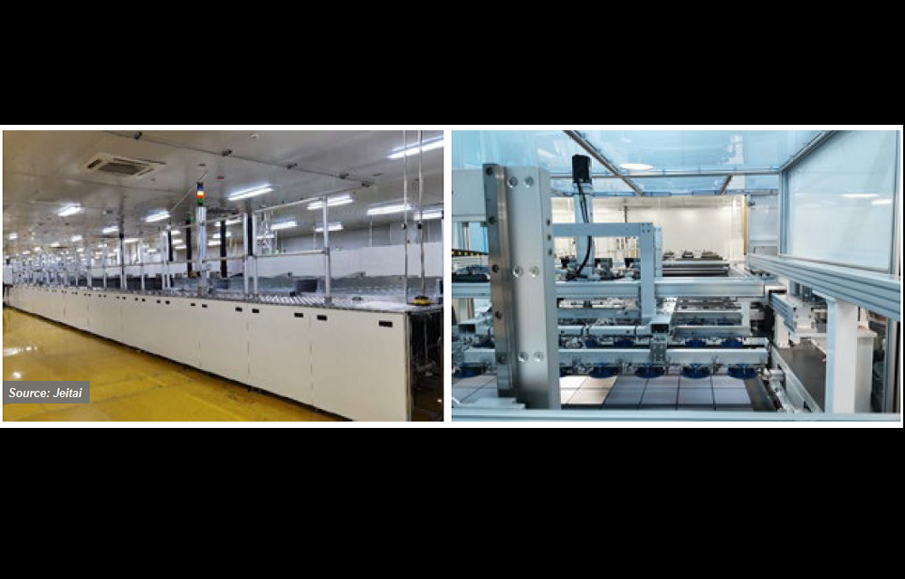
More than PVD: China’s Jietai has developed a hybrid technology platform called POPAID that essentially combines PVD and plasma oxidation to address the shortcomings of prevailing deposition technologies for TOPCon (Source: Jietai)
Technically falling under the PVD category, China-based Jietai prefers that its technology be called POPAID, which is short for Plasma Oxidation and Plasma Assisted In-situ Doping. Indeed, the technology is more than PVD; it combines PVD and plasma oxidation in one tool platform. Jiangsu Jietai Photoelectric Corp LTD (Jietai) has been working on solar equipment supply for about a decade now, with its initial focus on dry etching tools mainly designed for multicrystalline. In 2019, the company started working on its PVD based solution with an aim to address the shortcomings of other deposition technologies, especially wraparound. The company’s tool performs all necessary steps for TOPCon — formation of tunneling oxide, polysilicon deposition and in-situ doping.
The company uses linear RF plasma source for oxidation, which according to Jietai CEO Quanyuan Shang supports higher throughput, low damage and offers a higher degree of control. The throughput of the reactors is wafer size sensitive; it can process 10,000 G1 wafers per hour, dropping to 8,000 when processing M10 wafers. “The goal is to get 1 GW with two parallel lines (machines), that’s how we sized the tool,” said Shang. This throughput is at a polysilicon layer thickness of 100 nm. As one can expect, such a system is quite long, measuring 23 m in length. The tool has a scheduled maintenance cycle of 1 month, which the company is expecting to stretch to 2 months. Jietai is the equipment partner for Jolywood for its J-TOPCon 2.0 technology that is based on POPAID. Jietai has built one production tool so far and is expecting to ship POPAID tools of 5 GW by the end of this year, mainly to Jolywood. “We are pretty much sold out for this year,” said Shang. The company is ramping up its production facility, meaning it would honor the orders from others next year.
Polar PV seems to closely follow the reactor design of Jietai and presented its inline vertical magnetron sputtering PVD system in at a conference last year. The tool is designed to process a carrier with 60 cell slots in 6 x 10 configuration with a cycle time of 40 to 50 seconds. The tool is designed to accomplish all necessary steps for the TOPCon process; applying silicon oxide film, topped with in-situ doped polysilicon layer deposition. Even then the number of processing steps is considerably reduced compared to LPCVD. The reactor setup is equipped with a low energy oxygen plasma oxidation chamber for the formation of tunneling oxide in a pure gas plasma environment. The ionization source is also maintenance free. The amorphous silicon layer, deposited using rotary silicon targets and in-situ doping, is accomplished by the introduction of doping gas.
PVD has several advantages over the incumbent LPCVD. The first and foremost, according to Polar PV, is the low cost of operation and low maintenance. This cost saving stems from the fact that this process does not involve quartz-ware, which is a major cost driver for the LPCVD process. Moreover, being a single-side process, wraparound becomes less of an issue, further aiding cost savings. Polar PV’s PVD tool supports throughputs of up to 10,000 wafers per hour.
Energy consumption is another important means to reduce costs where the PVD shines through. Polar PV highlights that PVD uses 77% of the energy for coating and 16% for heating. In contrast, these figures are 34% and 45%, respectively, in the case of CVD. What this means is that energy utilization in PVD is far better than CVD, i.e., it is utilized where it matters more.
PVD also scores high in terms of process consumables. It uses silicon targets that are far cheaper than the silane used as the precursor in LPCVD. On the flip side, PVD has a high CapEx and a larger footprint.
Von Ardenne, with several decades of experience in building PVD reactors, has also been developing a TOPCon PV solution based on this technology. The German company’s solution for passivated contacts is based on sputtering of amorphous silicon on silicon oxide — still in the development phase, but with encouraging first results nonetheless. Once ready, Von Ardenne plans to implement the process on its high-throughput PVD tools platform, currently capable of processing over 10,000 wafers per hour.
As today the workhorse of the solar industry are still PERC cells, TaiyangNews will organize a virtual conference on Pushing PERC Cells to Its Limits on March 22, 2022.
Source from Taiyang News