- Recent developments in wet-chemistry related to PERC and HJT can also be applied for betterment of TOPCon
- BSG and single side emitter removal tools require TOPCon specific changes among the wet-benches
- Atmospheric dry etching technology from Nines photovoltaics aptly fits to requirements of removing wraparound from TOPCon cells
While the core of TOPCon lies in deposition of tunneling oxide and the polysilicon layer, producing these cells, similar to PERC, does require several processing steps that are worth mentioning, not critical though. Some of the processes that are part of the PERC process flow are tweaked or optimized, while altogether new steps are also required. Like with any other cell technology, TOPCon also starts with surface preparation, which requires some optimization.
Wet-chemical treatment: While not necessarily aimed at TOPCon alone, the key developments taking place in the wet-bench area can definitely benefit from the improvements made for other cell architectures. While two production tools need to be adapted for the TOPCon process – BSG and single-side emitter removal tools –, improvements with other wet-chemical treatment steps are also important in the larger scheme of things. RENA has been improving its tool platforms for the batch tools used for saw damage etching and texturing. Presenting at TaiyangNews High Efficiency Conference, RENA’s Kuhnlein mentioned that the most recent developments associated with these batch tools are the ability to accommodate larger wafers and process the carriers with high loading density. With improved wafer quality in general and developments in the field of additives, there is potential to eliminate the saw damage removal step from the PERC sequence altogether, which can also benefit TOPCon, according to Kuehnlein.
Another PERC development that can also help TOPCon is an optimized pyramid size and reflectivity. The current state of the art is a 1 to 3 µm pyramid size and 9.9 to 10.1% reflectivity with monoTEXH2.3. While there are approaches that can reduce the pyramid size from 0.5 to 3 µm and corresponding reflectivity of 8.9 to 10%, the latter is only achieved for a limited number of runs of about 20. RENA is working on a more stable process that can last for over 200 runs, realizing a pyramid size distribution of 0.5 to 2 µm and resulting in a reflectivity of about 9.3%.
RENA learned from its experience with HJT that cleaning after texturing has the potential to improve efficiency – up to 0.05% with PERC -, which can also be implemented in TOPCon processing.
In order to remove the wraparound, RENA is promoting an inline etching tool platform called InPolySide. During the alkaline single side etching step to strip the poly, the BSG on the emitter side of the cell prevents emitter etching and the process is precisely single sided, meaning the rear is left totally unaffected. After the stripping step, the glass is etched off.
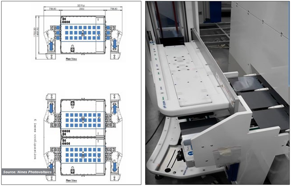
Atmospheric dry etching: As an alternative to the wet-chemical solutions to remove the wraparound, Nines Photovoltaics based out of Dublin, Ireland, is promoting an innovative solution. The company has developed a proprietary process called ADE, which stands for Atmospheric Dry Etching. The company has been developing the dry etching process since 2010 as a replacement for the typically used wet-chemical processes used in PV cell manufacturing. What makes this technology unique is that it accomplishes dry texturing at atmospheric pressure, eliminating the need for vacuum and plasma, which are both key ingredients and cost drivers in typical dry etching technologies, underscores Nines Photovoltaics’ CTO Laurent Clochard.
The reaction zone of the reactor is isolated from the rest by means of gas curtains. The process is accomplished in an inline fashion. The wafers are fed into the machines by means of a heated wafer carrier. An etching gas, which is fluorine (F2), is thermally activated in order to dissociate the molecules. The etchant is then delivered to the wafers through a specifically engineered distribution device in order to create the required etch depth, texture and uniformity. Clochard clarifies that the technology has no special adverse impact on the environment. The thought of fluorine as an etching gas itself rings alarm bells about greenhouse gases. However, unlike the commonly used SF6 with high global warming potential for dry etching, the molecular fluorine used by Nines has zero global warming potential.
The tool, when it was introduced in 2017, was mainly designed for texturing, to be specific, for multicrystalline, in which the gains in reflection ADE are way higher than what can be achieved with the state of the art wet-chemical solutions. However, with the market shifting to monocrystalline, Nines Photovoltaics also turned its focus to the mainstream PERC and other advanced technologies. While the technology still carried forward its advantages in texturing, the ADE found an even more appealing application in TOPCon cell processing. Given its single side nature of the process, it can be effectively used for the removal of wraparound. “What’s more?” says Clochard, “You can opt for surface etching and/or edge removal, as the technology is also selective.” That means Nines Photovoltaics’ process not only accomplishes the etching without disturbing the underlying emitter profile, but it can also be engineered to remove the polysilicon on wafer edges, which is the major contributor to the shunts and yield losses. The tool has application even when the deposition processes are single sided.
Nines is currently operating a pilot line at its facility in Dublin and has partnered with Fraunhofer ISE for cell process development while also having supplied an R&D-scale system. The company is now ready with the production-scale platform, which is offered in 2 variants – ADE-3000 and ADE-6000. The latter processes wafers up to a size of M4 in six lanes and M6 to G12 in 4 lanes. The tool has a rated throughput of 12,000 and 8,000 wafers per hour, respectively, in a footprint of 12 m2. The number of lanes is exactly half with ADE-3000, so is the throughput. These throughputs figures, however, are for to the texturing process, meaning the tool capacity would be much higher for single-side etching in TOPCon. “The amount of silicon that needs to be removed 10 times less than what you would for texturing,” explains Clochard. The company is also willing to supply an R&D scale system with single lane of transport. As for costs, Clochard says that the costs are considerably lower than wet-chemical processes and the benefits are more apparent in larger scale production. This is facilitated by the fact that the etching gas can be produced on-site, according to Clochard.
Source from Taiyang News